P54TS/P54TSW/P54TSW2 Motherboard Settings and Configuration
QUICK TECHNOLOGY, INC.
P54TS/P54TSW/P54TSW2
Processor | Pentium |
Processor Speed | 75/90/100/120/133/150/166/180/200MHz |
Chip Set | Intel |
Max. Onboard DRAM | 128MB |
Cache | 256/512KB |
BIOS | Award |
Dimensions | 330mm x 220mm |
I/O Options | 32-bit PCI slots (3), floppy drive interface, green PC connector, IDE interfaces (2), wide SCSI-2 connector, fast SCSI-2 connector, parallel port, PS/2 mouse interface, serial ports (2), VRM connector, cache slot |
NPU Options | None |
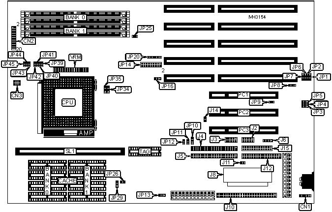
CONNECTIONS | |||
Purpose | Location | Purpose | Location |
PS/2 mouse interface | CN1 | IDE interface 2 | J5 |
Speaker | CN2 pins 1 - 4 | Wide SCSI-2 interface | J8 |
Power LED & keylock | CN2 pins 6 - 10 | Fast SCSI-2 interface | J10 |
Reset switch | CN2 pins 11 & 12 | SCSI-2 interface LED | J11 |
Turbo switch | CN2 pins 13 & 14 | Floppy drive interface | J12 |
Green PC connector | CN2 pins 16 & 17 | IDE interface LED | J14 |
Turbo LED | CN2 pins 18 & 19 | Parallel port | J15 |
Chassis fan power | CN3 | 32-bit PCI slots | PC1 - PC3 |
Serial port 1 | J2 | Cache slot | SL1 |
Serial port 2 | J3 | VRM connector | VRM |
IDE interface 1 | J4 | ||
Note: J8 is not on the P54Ts board. | |||
USER CONFIGURABLE SETTINGS | |||
Function | Jumper | Position | |
Factory configured - do not alter | J6 | N/A | |
» | Factory configured - do not alter | JP1 | pins 2 & 3 closed |
» | Factory configured - do not alter | JP2 | pins 1 & 2 closed |
» | Printer EPP mode IRCHRDY signal enabled | JP5 | pins 1 & 2 closed |
Printer EPP mode IRCHRDY signal disabled | JP5 | pins 2 & 3 closed | |
» | Factory configured - do not alter | JP6 | N/A |
» | Factory configured - do not alter | JP7 | N/A |
» | Parallel port IRQ select IRQ7 | JP8 | pins 1 & 2 closed |
Parallel port IRQ select IRQ5 | JP8 | pins 2 & 3 closed | |
» | Enhanced multi I/O enabled | JP9 | Open |
Enhanced multi I/O disabled | JP9 | Closed | |
» | SCSI chip enabled | JP10 | pins 1 & 2 closed |
SCSI chip disabled | JP10 | pins 2 & 3 closed | |
Primary IDE IRQ14 enabled | JP11 | pins 1 & 2 closed | |
Primary IDE IRQ14 disabled | JP11 | pins 2 & 3 closed | |
Secondary IDE IRQ15 enabled | JP12 | pins 1 & 2 closed | |
Secondary IDE IRQ15 disabled | JP12 | pins 2 & 3 closed | |
» | SCSI terminator control select controlled by BIOS | JP13 | pins 2 & 3 closed |
SCSI terminator control select always on | JP13 | pins 1 & 2 closed | |
SCSI terminator control select always off | JP13 | Open | |
BIOS type select EPROM | JP20 | pins 2 & 3, 4 & 5 closed | |
BIOS type select 5v flash | JP20 | pins 2 & 3, 5 & 6 closed | |
BIOS type select 12V flash | JP20 | pins 1 & 2, 5 & 6 closed | |
» | Factory configured - do not alter | JP25 | N/A |
» | SCSI-2 enabled | JP26 | Open |
Wide SCSI-2 enabled | JP26 | Closed | |
DRAM CONFIGURATION | ||
Size | Bank 0 | Bank 1 |
2MB | (2) 256K x 36 | NONE |
4MB | (2) 512K x 36 | NONE |
4MB | (2) 256K x 36 | (2) 256K x 36 |
6MB | (2) 512K x 36 | (2) 256K x 36 |
6MB | (2) 256K x 36 | (2) 512K x 36 |
8MB | (2) 1M x 36 | NONE |
8MB | (2) 512K x 36 | (2) 512K x 36 |
10MB | (2) 1M x 36 | (2) 256K x 36 |
10MB | (2) 256K x 36 | (2) 1M x 36 |
12MB | (2) 1M x 36 | (2) 512K x 36 |
12MB | (2) 512K x 36 | (2) 1M x 36 |
16MB | (2) 2M x 36 | NONE |
16MB | (2) 1M x 36 | (2) 1M x 36 |
18MB | (2) 2M x 36 | (2) 256K x 36 |
18MB | (2) 256K x 36 | (2) 2M x 36 |
20MB | (2) 2M x 36 | (2) 512K x 36 |
20MB | (2) 512K x 36 | (2) 2M x 36 |
24MB | (2) 2M x 36 | (2) 1M x 36 |
24MB | (2) 1M x 36 | (2) 2M x 36 |
32MB | (2) 4M x 36 | NONE |
32MB | (2) 2M x 36 | (2) 2M x 36 |
34MB | (2) 4M x 36 | (2) 256K x 36 |
34MB | (2) 256K x 36 | (2) 4M x 36 |
36MB | (2) 4M x 36 | (2) 512K x 36 |
36MB | (2) 512K x 36 | (2) 4M x 36 |
40MB | (2) 4M x 36 | (2) 1M x 36 |
40MB | (2) 1M x 36 | (2) 4M x 36 |
48MB | (2) 4M x 36 | (2) 2M x 36 |
48MB | (2) 2M x 36 | (2) 4M x 36 |
64MB | (2) 8M x 36 | NONE |
64MB | (2) 4M x 36 | (2) 4M x 36 |
66MB | (2) 8M x 36 | (2) 256K x 36 |
66MB | (2) 256K x 36 | (2) 8M x 36 |
68MB | (2) 8M x 36 | (2) 512K x 36 |
68MB | (2) 512K x 36 | (2) 8M x 36 |
72MB | (2) 8M x 36 | (2) 1M x 36 |
72MB | (2) 1M x 36 | (2) 8M x 36 |
80MB | (2) 8M x 36 | (2) 2M x 36 |
80MB | (2) 2M x 36 | (2) 8M x 36 |
96MB | (2) 8M x 36 | (2) 4M x 36 |
96MB | (2) 4M x 36 | (2) 8M x 36 |
128MB | (2) 8M x 36 | (2) 8M x 36 |
CACHE CONFIGURATION | ||||
Size | Bank 0 | Bank 1 | TAG | SL1 |
256KB (A) | (4) 32K x 8 | (4) 32K x 8 | (1) 8K x 8 | Not installed |
256KB (B) | NONE | NONE | NONE | Installed |
512KB (A) | (4) 64K x 8 | (4) 64K x 8 | (1) 16K x 8 | Not installed |
512KB (B) | NONE | NONE | NONE | Installed |
Note: If SL1 is used, chips must be removed from Banks 0 & 1 and TAG. | ||||
CACHE JUMPER CONFIGURATION | |
Size | JP29 |
256KB | pins 1 & 2 closed |
512KB | pins 2 & 3 closed |
CACHE TYPE CONFIGURATION | ||
Type | JP34 | JP35 |
Asynchronous | pins 1 & 2 closed | pins 2 & 3 closed |
Burst | pins 2 & 3 closed | pins 1 & 2 closed |
Pipeline burst | pins 1 & 2 closed | pins 1 & 2 closed |
CPU TYPE CONFIGURATION | |
Type | JP16 |
P54C/CS/CT | pins 1 & 2 closed |
P55C/CT | pins 2 & 3 closed |
CPU SPEED CONFIGURATION | |
Speed | JP14 |
75MHz | pins 1 & 2 closed |
90MHz | pins 3 & 4 closed |
100MHz | pins 5 & 6 closed |
120MHz | pins 7 & 8 closed |
133MHz | pins 9 & 10 closed |
150MHz | pins 11 & 12 closed |
166MHz | pins 13 & 14 closed |
180MHz | pins 15 & 16 closed |
200MHz | pins 17 & 18 closed |
CPU VOLTAGE CONFIGURATION | ||||
» Voltage | JP43 | JP44 | JP45 | |
| » | 3.4v | Open | Open | Closed |
| » | 3.5v | Open | Closed | Open |
| » | 3.6v | Closed | Open | Open |
VRM CONFIGURATION | |||||
» Setting | JP39 | JP40 | JP41 | JP42 | |
| » | VRM not installed | Closed | Closed | Closed | Closed |
| » | VRM installed | Open | Open | Open | Open |
DMA CONFIGURATION | |||
» DMA | JP3 | JP4 | |
| » | DMA 1 | pins 1 & 2 closed | pins 1 & 2 closed |
| » | DMA 3 | pins 2 & 3 closed | pins 2 & 3 closed |


My Books